The Interface: Cognichip Blog
ACI Enterprise — 25 Years of Margin Sketches
September 28, 2026
By: Stelios Diamantidis
Chief Product Officer
There are moments in a career when the work in front of you finally matches the picture you've carried in your head for decades. For me, now is one of those moments.
I've spent more than 25 years in and around chip design — as an engineer, a founder, an executive, and, for the past decade, as someone convinced that artificial intelligence would fundamentally change how silicon gets made. I've built companies, launched the industry's first AI application for chip design, and watched brilliant teams push against the limits of what our tools could do. And through all of it, I kept sketching the same product in the margins: a system that didn't just assist chip designers here and there, but that truly ‘talked chip’ — one that could carry an idea from a rough specification all the way to working silicon at something close to the speed of software.
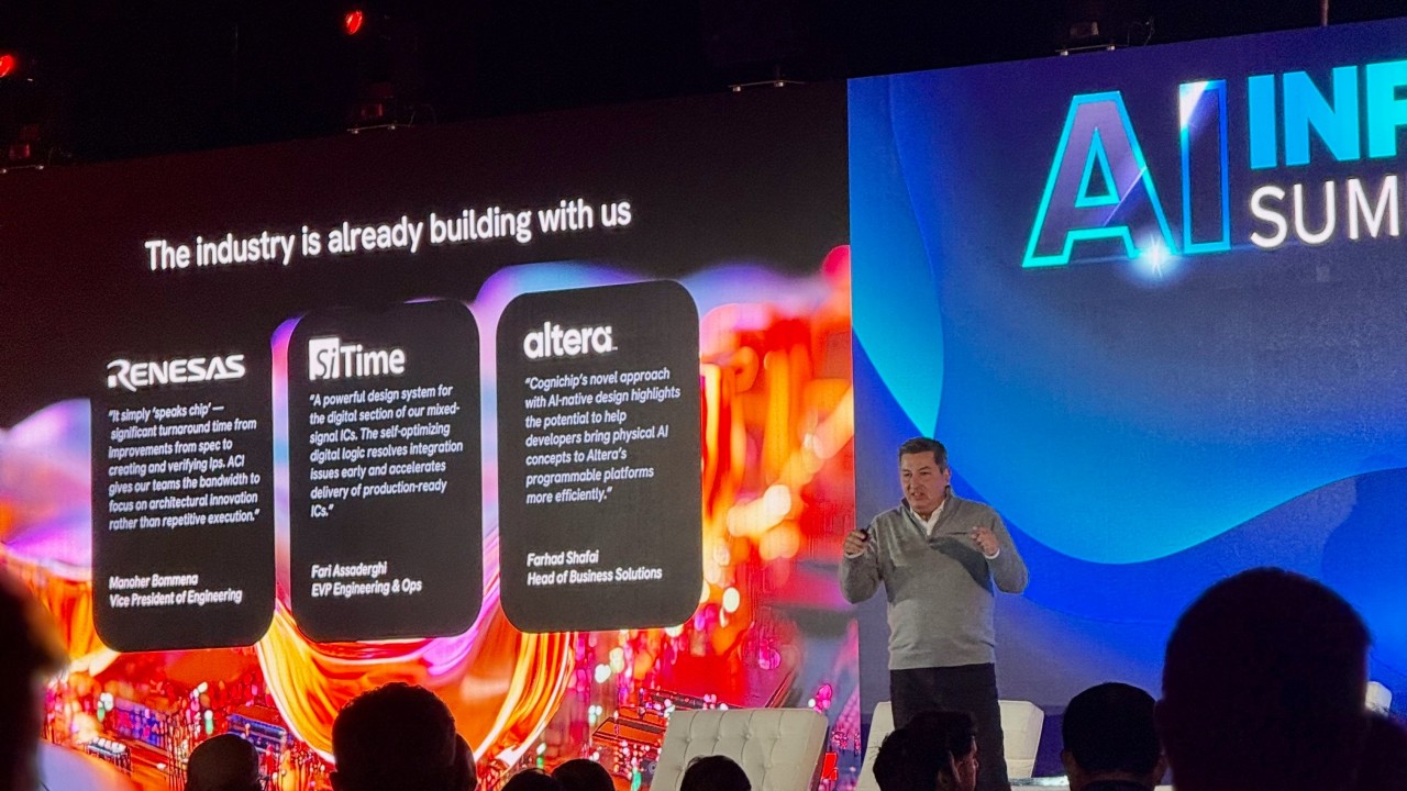
That product is here. At AI Infra Summit 2026, we announced ACI Enterprise, the world's first full-stack intelligence infrastructure for chip design. I could not be prouder of what our team has built.
Let me tell you why this matters to me personally, and why I believe it matters to our industry.
Why ACI?
Chip design has become extraordinary and, frankly, unsustainable. A single advanced-node tape-out can cost between $40 and $100 million. The industry is staring down a shortage of more than a million skilled designers by the end of the decade. And most painful of all: our talented engineers spend roughly 95% of their time on execution — the necessary, repetitive grind — and only a sliver on the architectural creativity that drew them to this field in the first place. We have been rationing innovation.
Our talented engineers spend 95% of their time on execution — we have been rationing innovation.
I've felt that constraint my whole career. Artificial Chip Intelligence ACI™ is our answer to it.
We made a deliberate bet early on: that general-purpose language models, however impressive, would never possess the rigor and mathematical precision chip engineering demands. So, we built something native to our domain.
ACI Enterprise — four industry firsts in one system
First, physics-informed foundation models purpose-built for chip design. Rather than bolting design logic onto a general model with clever wrappers, we grounded our models in semiconductor physics and trained them on the industry's largest dataset — over 3M datasets developed by engineers who have collectively shipped hundreds of chips and scientists who have four World Olympiad medals and over 40,000 citations to their name. This design intelligence lives inside the models themselves, which is why ACI converges with high accuracy and efficiency.
Median APE % by PPA metric
Lower is better · median absolute % error on 1,232 GitHub repos
Second, a full-stack intelligence infrastructure. ACI unifies workflows, an agent framework, context and memory, compute and inference, and proprietary data into a single self-learning flywheel — applying the right density of intelligence to the right task, while giving customers native control over data residency, deployment, customization, and cost.
Third, AI-native workflows built on a simple but radical idea: the model IS the design. Specifications, RTL, tests, constraints, and performance all live together in one living, evolving model. ACI analyzes specs, generates and formally verifies RTL, drives verification through to closure, debugs and fixes issues, and optimizes power, performance, and area to the Pareto limit.
Fourth, hardware innovation at software speed for physical AI. ACI takes designs from idea to working FPGA implementation, lowering the technical and financial barriers for a new generation of builders — in 5G infrastructure, autonomous automotive systems, industrial IoT — to create sophisticated custom silicon without the traditionally steep learning curve of FPGA design.
With ACI, the model IS the design.
What moves me most isn't one standout project or a single astounding result of many — it's the consistency. Over the past several months of working closely with our early partners, I've seen the same pattern again and again: efforts that once stretched across months now come together in a matter of days. It holds true across wildly different design styles and architectures, across every level of experience, and across companies of every size, from stealth-mode startups to top-20 semiconductor leaders. This is not a step change in speed. It is a fundamental rewrite of the way we design chips.
Arch. Exploration
~5× faster · working days
RTL Design
~5× faster · working days
Testbenches & Debug
~7× faster · working days
UVM Closure
~20× faster · working days
And we did it without asking anyone to compromise on what matters most — their intellectual property. A customer's design “alpha,” the architectural intuition that makes them who they are, stays inside their environment. Cognichip can account for every spec fragment, every gate, every transistor, and every metric that is used to train our models. Your data will never find its way into Cognichip's training pipelines. Conversely, other peoples' data will never find its way into yours. Full stop.
A customer's design “alpha,” your data, will never find its way into Cognichip's training pipelines.
A new era of semiconductor engineering starts now
Here's the part that makes me the most proud. For two and a half years, an extraordinary group of people poured themselves into a problem that many told us was impossible. To our chip designers and scientists, who taught our models what decades of hard-won expertise feels like — thank you. To our software and security engineers, who turned deep research into infrastructure that enterprises can trust — thank you. To our product team, who sat with customers, listened, and carried their reality back to us every single day — thank you. To our people and finance teams, who built the culture that made all of this possible — thank you. Your fingerprints are on every part of this product.
Finally, to our executive team, board members Lip-Bu Tan, Umesh Padval, Shahin Farshchi, and investors Seligman Ventures, SBI Investment, Mayfield, Lux Capital, FPV Ventures and Candou Ventures: it is a genuine privilege to work alongside you. I learn from you constantly, and I'm grateful for it.
And to our customers and partners — including the teams at Renesas Electronics, SiTime, and Altera who trusted us early, when trust was the hardest thing to ask for — you have shaped this product as much as anyone inside our walls.
Twenty-five years ago, I couldn't have imagined a system like ACI. Ten years ago, I hoped for it. Two and a half years ago, we started building it. Now, we get to share it with the world.
This is the product I've always wanted to bring to market — not because it's finished (the best is genuinely ahead of us), but because of what it frees people to do. If we've done our jobs well, chip designers everywhere will spend a little less time on the grind and a lot more time on the ideas that only they can dream up.
What will YOU design today?
— Stelios
By: Stelios Diamantidis
Chief Product Officer

